K230 DEMO BOARD Resource Usage Instructions#
disclaimer#
The products, services or features you purchase should be subject to Canaan Inc. (“Company”, hereinafter referred to as “Company”) and its affiliates are bound by the commercial contracts and terms and conditions of all or part of the products, services or features described in this document may not be covered by your purchase or use. Unless otherwise agreed in the contract, the Company does not provide any express or implied representations or warranties as to the correctness, reliability, completeness, merchantability, fitness for a particular purpose and non-infringement of any statements, information, or content in this document. Unless otherwise agreed, this document is intended as a guide for use only.
Due to product version upgrades or other reasons, the content of this document may be updated or modified from time to time without any notice.
Trademark Notice#
 , “Canaan” and other Canaan trademarks are trademarks of Canaan Inc. and its affiliates. All other trademarks or registered trademarks that may be mentioned in this document are owned by their respective owners.
Copyright 2023 Canaan Inc.. © All Rights Reserved. Without the written permission of the company, no unit or individual may extract or copy part or all of the content of this document without authorization, and shall not disseminate it in any form.
directory#
[TOC]
preface#
overview#
THIS DOCUMENT MAINLY INTRODUCES THE INSTRUCTIONS FOR USING THE K230 DEMO BOARD.
Reader object#
This document (this guide) is intended primarily for:
Technical Support Engineer
Software Development Engineer
Definition of acronyms#
abbreviation |
illustrate |
|---|---|
Revision history#
Document version number |
Modify the description |
Modified by |
date |
|---|---|---|---|
V1.0 |
first edition |
Du Lingyi |
2023-03-10 |
V1.1 |
Changed to the description corresponding to EVB V1.1 |
Du Lingyi |
2023-05-05 |
V1.2 |
Updated J5, USB OTG pin header |
Du Lingyi |
2023-05-10 |
V1.3 |
CHANGE THE CONTENT FROM EVB TO K230 DEMO BOARD |
Du Lingyi |
2023-06-07 |
Overview of the development board#
K230 DEMO BOARD概要#
The K230 DEMO BOARD is a complete development test board with a camera daughter board and screen, which is already in the plug-and-play state, and the follow-up development work for the K230 can be started after powering on. The K230 DEMO BOARD will be delivered as a motherboard assembly with multiple daughter boards. THIS DOCUMENT WILL BRIEFLY SUMMARIZE THE COMPONENT DAUGHTER BOARDS AND USAGE PROCESS OF THE K230 DEMO BOARD through various interfaces on the motherboard.
Schematic diagram of the K230 DEMO BOARD motherboard#
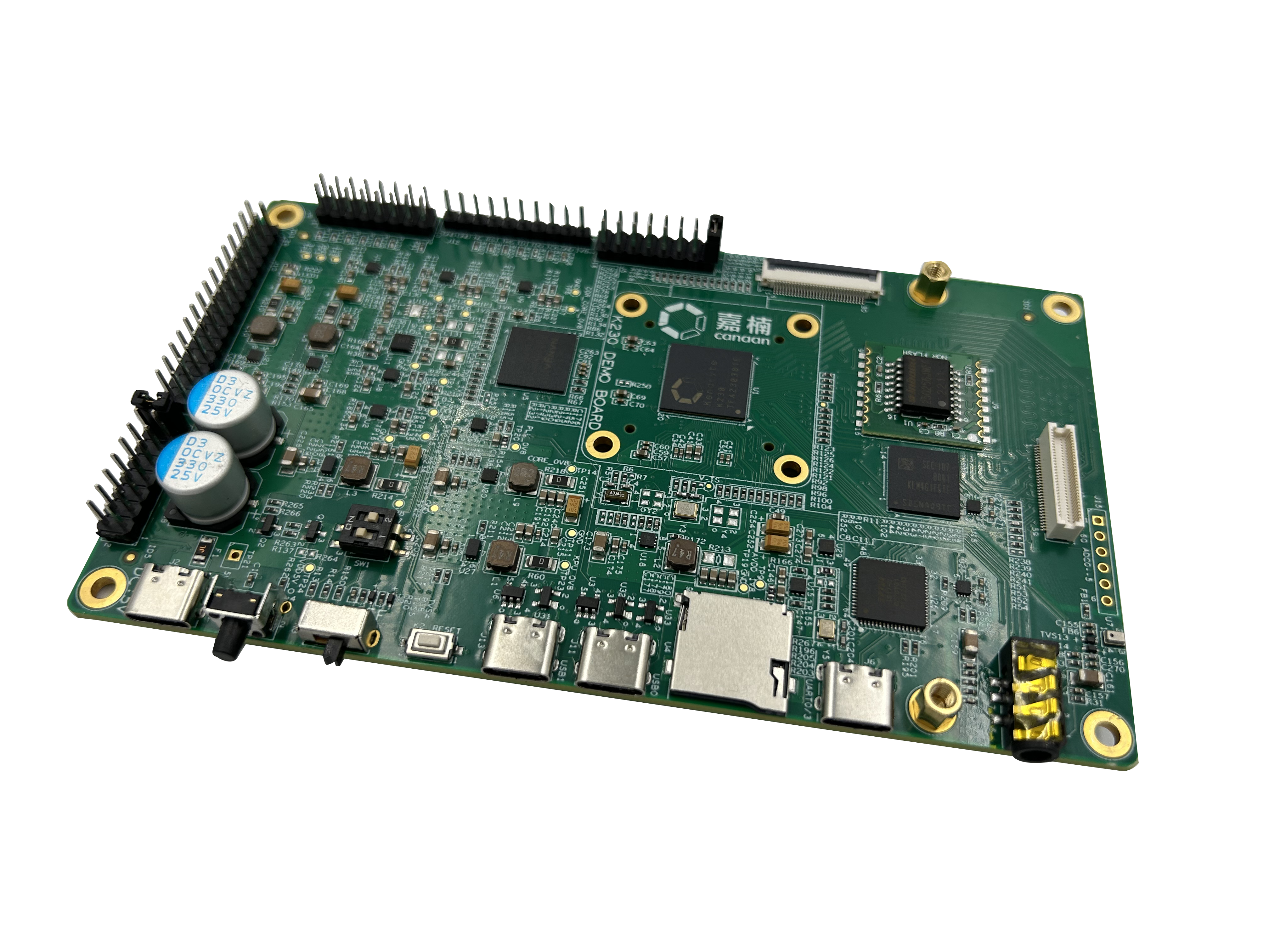 (Figure 1.2.1: Example of a K230 DEMO BOARD sample, daughter plate not assembled).
K230 DEMO BOARD is equipped with assembly daughter boards#
To ensure verification flexibility, the K230 DEMO BOARD is equipped with a variety of interfaces and the ability to communicate with different types of daughter cards for more comprehensive development of chip functions. The types of daughter boards that can be equipped with the motherboard are as follows:
Flash module daughter card (see Section 2.2 for details).
Screen and DSI interposer board (see Section 2.4 for details).
IMX335 Module Sensor Board (see Section 2.4 for details).
WIFI daughter card (see Section 2.6 for details).
I2S/PDM interface digital audio daughter card (see Section 2.7 for details).
The use of interfaces and daughter cards is described in detail when describing the interfaces corresponding to the daughter card in Chapter 2**. Among the above daughter cards, Flash module daughter card, DSI screen and adapter board, IMX335 module Sensor board will be assembled on the K230 DEMO BOARD motherboard for delivery, and the remaining daughter cards are not included in the delivery list of the K230 DEMO BOARD by default, and are listed here only to assist in illustrating the relevant interface functions and usage.
IN ADDITION, THE FOLLOWING DEVELOPMENT CABLES ARE INCLUDED WHEN DELIVERED USING THE K230 DEMO BOARD:
2 USB Type C cables
OTG adapter, Type C male to USB-A female 1
Type C male to network port cable 1
To assemble the complete DEMO board, please refer to Figure 1.3.1
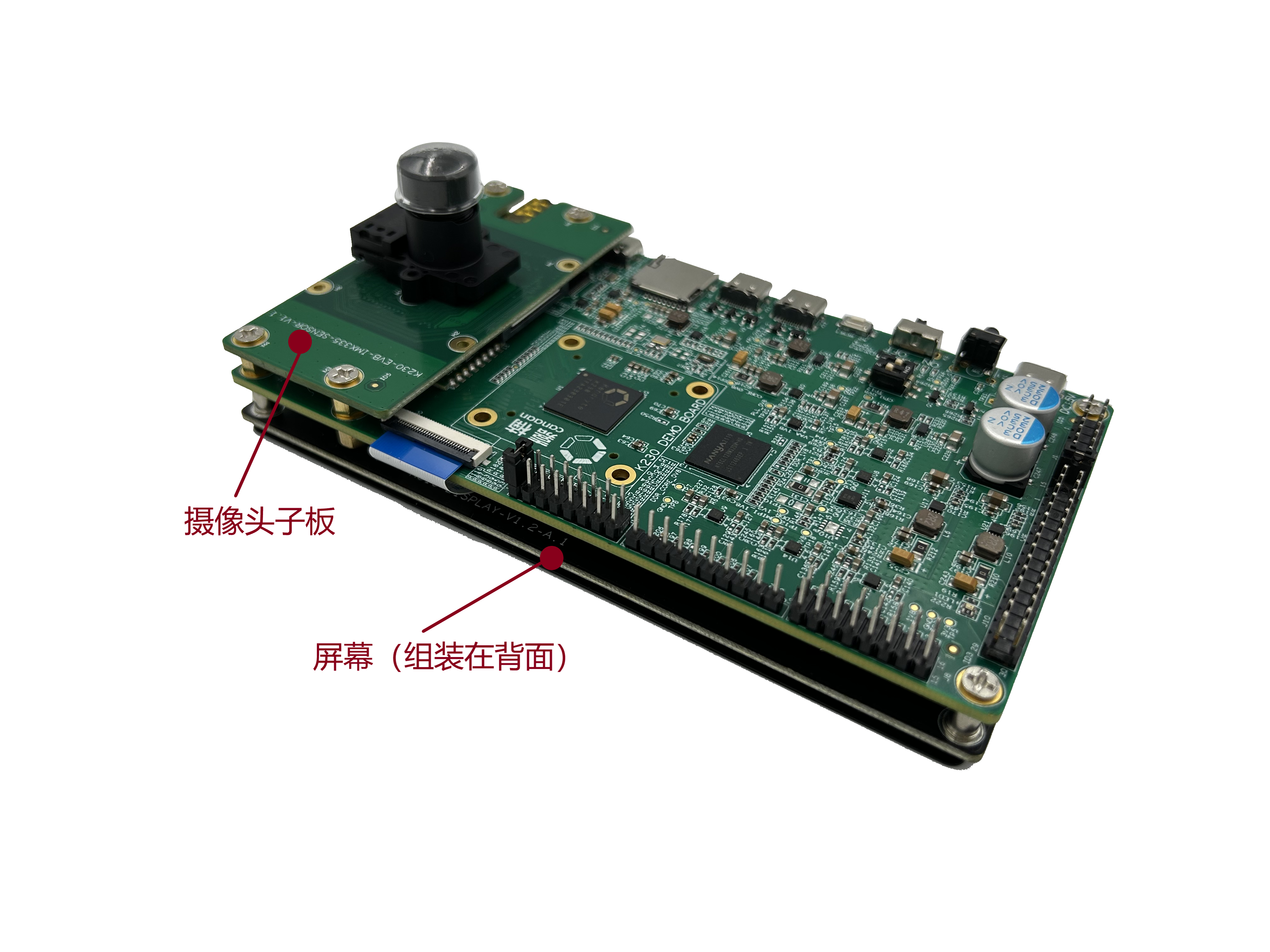 (Figure 1.3.1: Example of K230 DEMO BOARD sample, fully assembled).
DEMO BOARD HARDWARE FUNCTION DESCRIPTION#
K230 DEMO BOARD motherboard function module and all interfaces#
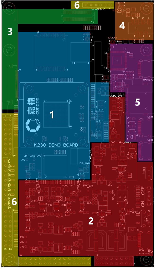
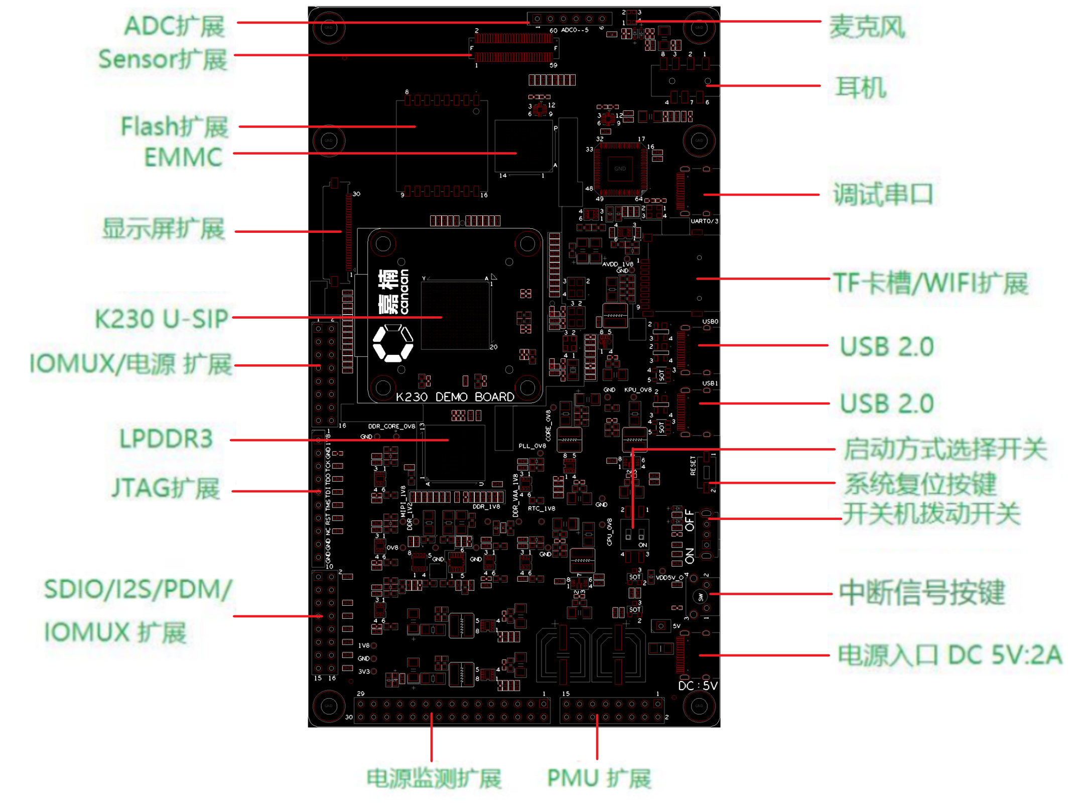 (FIGURE 2.1.1: THE UPPER FIGURE IS THE FUNCTIONAL AREA DIVISION OF THE K230 DEMO BOARD, AND THE FOLLOWING FIGURE SHOWS ALL THE SUPPORTED INTERFACES AND THEIR CORRESPONDING POSITIONS ON THE DEMO BOARD).
The K230 DEMO BOARD can be roughly divided into 6 regions as shown in the left figure in Figure 2.1.1, in the order of the serial number:
(Blue) Core Area - This is where the main chip K230 and its storage DDR, flash, eMMC, and system master clock are located.
(Red) Power Zone - That is, the location of all power supplies on the DEMO BOARD motherboard and power control devices.
(Green) Video Zone - This is where the camera is connected to the screen and motherboard.
(Orange) Audio Zone - This is where the microphone and headphones are located.
(purple) Generally Interface – Interface area for data exchange with other devices.
(Yellow) Pin header – This area contains pins corresponding to critical signals on the DEMO BOARD, which can be used as test points or connection points to external signals, expansion daughter cards, etc.
Each region in the figure on the left contains several devices/interfaces listed in the figure on the right. The devices/interfaces covered in each area are displayed in the following order in the following sections of this section. If necessary, additional information or instructions on how to use the corresponding device/interface will be displayed.
In the case of schematic diagrams in this section, unless otherwise specified, the pins of the device package on the DEMO BOARD are exactly the same as the package pins on the schematic (referring to single and double rows, pin out order). In addition, all pin numbers mentioned and device numbers are indicated on the K230 DEMO BOARD through white silkscreen, please confirm in conjunction with the DEMO BOARD.
Core area (basic parameters)#
THIS PART IS THE CORE PROCESSING AND STORAGE AREA OF THE DEMO BOARD, INCLUDING THE FOLLOWING FIVE INTERFACES/DEVICES LISTED IN THE RIGHT FIGURE OF FIGURE 2.1.1
K230-USIP (DEMO BOARD PART NUMBER: U1)
LPDDR3 (DEMO BOARD PART NUMBER: U5). The selection is NT6CL128M32DM-H0, Nanya 32bits - 4Gbits lpddr3, and support 2133Mbps
eMMC (DEMO BOARD: U30). Selected as KLM4G1FETE-B041, Samsung 8bits - 4GBytes eMMC, compatible with Ver. 5.1, clock rate 200MHz
Flash Extension (Part No. J9 on DEMO BOARD)
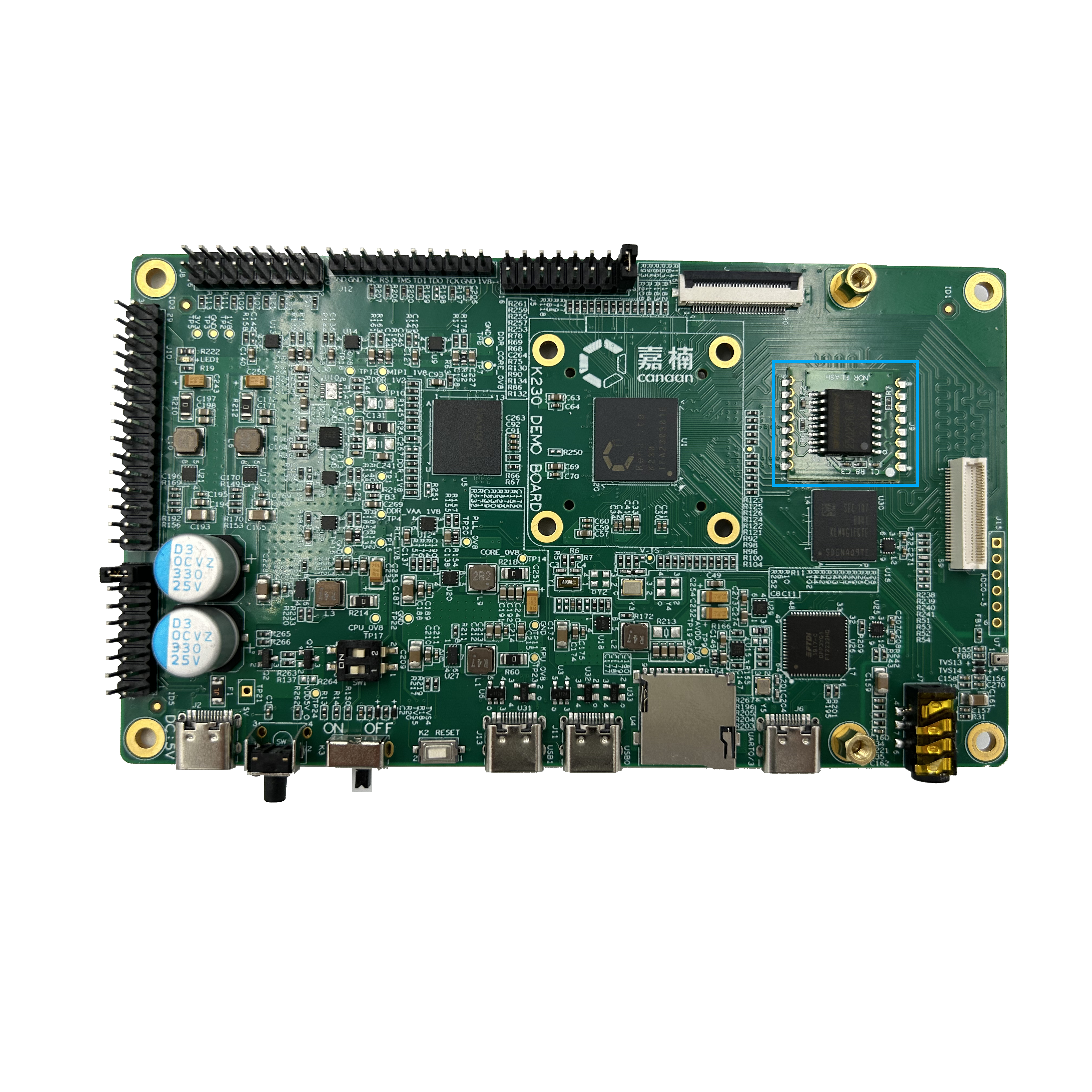 of the flash module daughter card
 (Figure 2.2.1: The above figure is an example diagram of the flash module daughter card, pin 1 is at the upper left white point, and the following figure is the schematic of Flash Extension-J9).
THE EXTENSION OF THE FLASH OF THE DEMO BOARD HAS BEEN WELDED WITH THE VERIFIED FLASH MODULE, AND NO FURTHER CHANGES ARE REQUIRED. The selection is NOR flash OSPI interface(GD25LX256E, manufacturer: Giga Device, 256Mbits)
Power zone (power-on mode)#
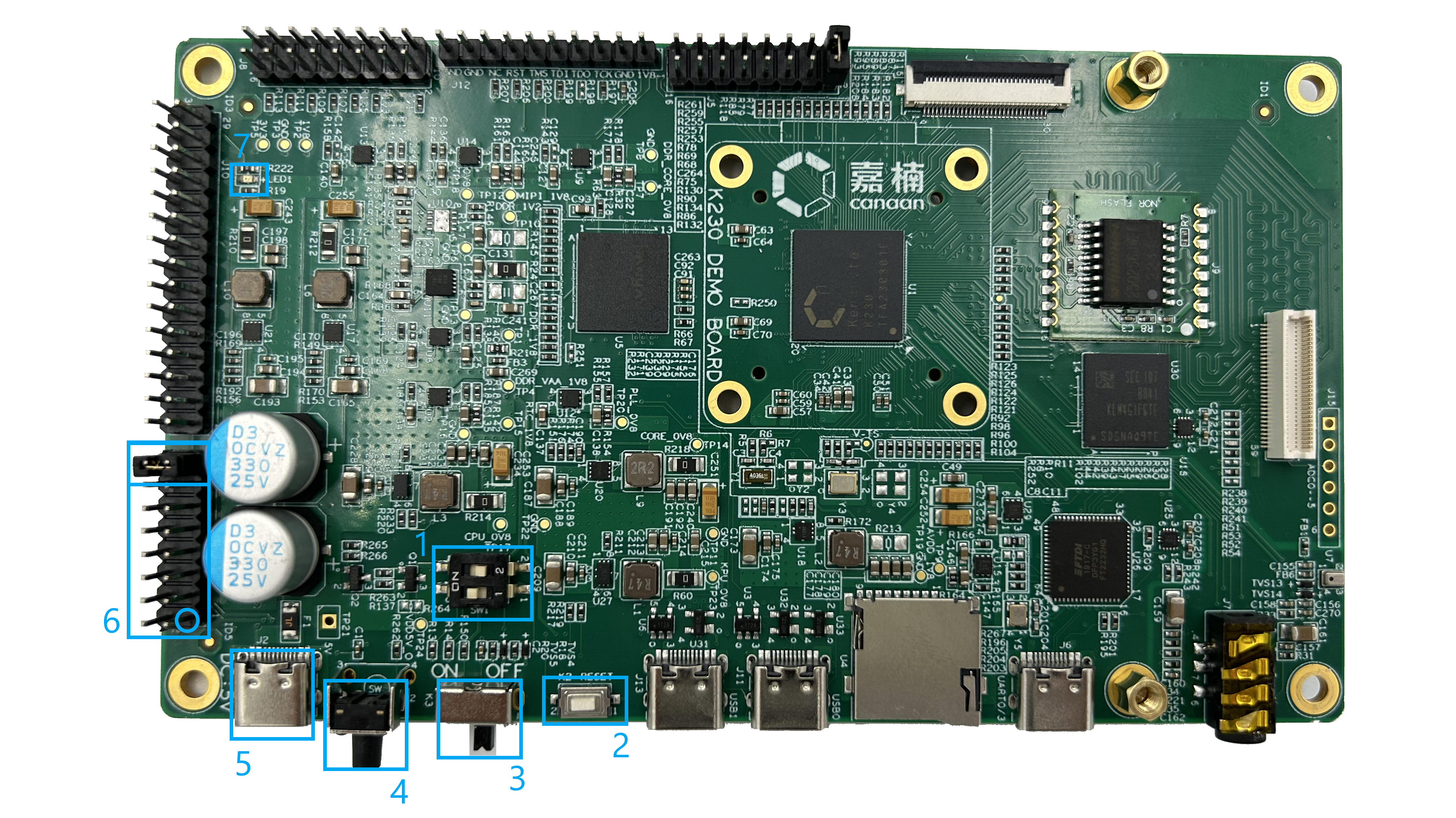
(Figure 2.3.1: Location of the main device in the power region, shown in the mode of power-up through the switch).
THIS AREA GENERATES ALL THE POWER NEEDED ON THE DEMO BOARD. ALL INTERACTIVE DEVICES RELATED TO THE DEMO BOARD POWER CONTROL ARE LOCATED IN THIS AREA, AND THERE ARE 2 POWER-ON MODES TO CHOOSE FROM (SELECTION WILL BE EXPLAINED LATER). The numbers in Figure 2.3.1 correspond to the following six main interfaces/devices (names are consistent with the list in the right figure in Figure 2.1.1).
START-UP OPTION SELECTOR SWITCH (PART NUMBER SW1 ON DEMO BOARD). The K230 supports loading boot files from four different places, and a DIP switch to select the K230’s startup position through four high and low states. For the schematic diagram of the startup position and SW1 corresponding to the four states, please refer to Figure 2.3.2 below.
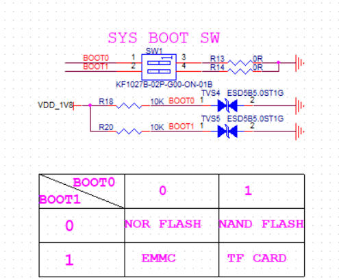 (Figure 2.3.2: SW1 schematic)
Among them, switches 1 and 2 correspond to BOOT0 and BOOT1 respectively. DIAL THE SWITCH TO PIN 1, 2 CORRESPONDS TO HIGH LOGIC 1 (THE H SIDE MARKED ON THE DEMO BOARD), AND TO PIN 3, 4 CORRESPONDS TO LOW LOGIC 0 (THE L SIDE MARKED ON THE DEMO BOARD). The above numbers are indicated by silkscreen on the DEMO BOARD board.
(Figure 2.3.2: SW1 schematic)
Among them, switches 1 and 2 correspond to BOOT0 and BOOT1 respectively. DIAL THE SWITCH TO PIN 1, 2 CORRESPONDS TO HIGH LOGIC 1 (THE H SIDE MARKED ON THE DEMO BOARD), AND TO PIN 3, 4 CORRESPONDS TO LOW LOGIC 0 (THE L SIDE MARKED ON THE DEMO BOARD). The above numbers are indicated by silkscreen on the DEMO BOARD board.**SYSTEM RESET BUTTON (PART NUMBER ON DEMO BOARD: K2). Low valid key reset. Pull the reset low when pressed, and the normal high level when released. The current reset condition can be determined by sensing the voltage at pin 2.
SWITCH ON AND OFF TOGGLE SWITCH (PART NUMBER ON DEMO BOARD: K3)
Interrupt signal button (PART NUMBER ON DEMO BOARD: K1) Test keys for manual interrupt generation.
Power Inlet DC 5V: 2A (PART NUMBER ON DEMO BOARD: J2)
PMU EXTENSION (PART NUMBER ON DEMO BOARD: J1) The pin header extensions used for power supply testing are not required when using the DEMO board.
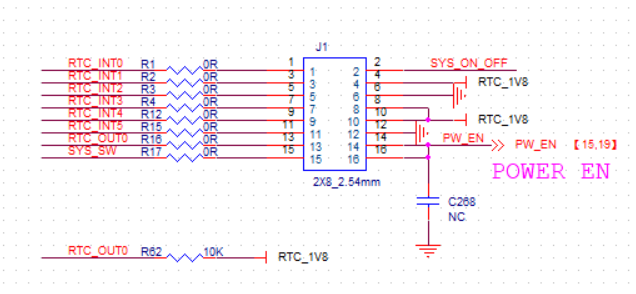 (Figure 2.3.3:P MU extension J1 schematic).
RED LED POWER INDICATOR (PART NUMBER ON DEMO BOARD: LED1)
The normal boot process is as follows:
Dial SW1 to the desired BOOT position
Connect the 5V voltage to the power inlet-J2 through the Type-C power cable.
Toggle K3 to the ON position to power on. If the power supply is successfully applied, the red LED in Figure 2.3.1 will illuminate
In the case of good power, you can ensure that the K230 starts successfully by checking whether the reset status is high.
If the power LED does not light up when powering on the system, verify that the jumper caps at pins 15 and 16 of the PMU extension (J6) (i.e., the locations additionally indicated in the box numbered 6 in Figure 2.3.1) are properly seated.
Video input and output (camera daughter board and screen daughter board)#
 (Figure 2.4.1: Main device locations in the video region).
THE CONNECTION BETWEEN THE CAMERA AND THE SCREEN DAUGHTER CARD DELIVERED WITH THE DEMO BOARD. The numbers in Figure 2.4.1 correspond to the following two main interfaces/devices (the names match the list in the right figure in Figure 2.1.1).
DISPLAY EXTENSION (PART NUMBER ON DEMO BOARD: J4). The interface of MIPI DSI is to transmit video signals sent from MIPI to the display screen through the FPC cable, also known as MIPI TX interface. Here is the connection of the DSI touch screen adapter board in the list described in Section 1.3, and J4 and the adapter board can be directly connected through the 30Pin-wide FPC cable. The pin definition schematic for J4 is shown in Figure 2.4.2.
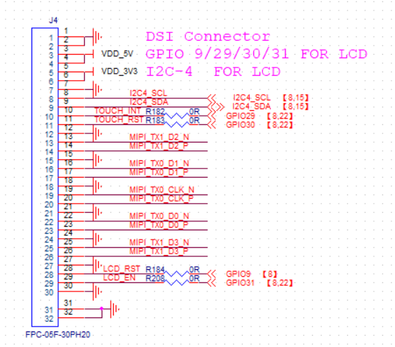 (Figure 2.4.2: Display expansion pin definition schematic, pins 31, 32 are fixed pins are not signal pins, can be ignored).
Sensor extension (part number J3 on DEMO BOARD). The interface of MIPI CSI is to transmit the video signal received from the camera by MIPI through a board-to-board connector, also known as the MIPI RX interface. Here is the connection of the IMX335 module Sensor board in the list described in Section 1.3. The pin definition schematic for J3 is shown in Figure 2.4.3.
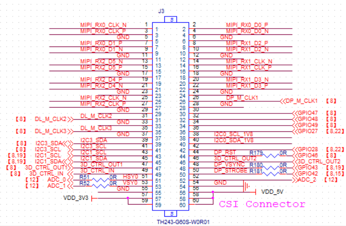 (Figure 2.4.3: Sensor expansion pin definition schematic).
All module daughter boards are assembled at the time of delivery, as shown in Figure 1.3.1.
Audio input and output#
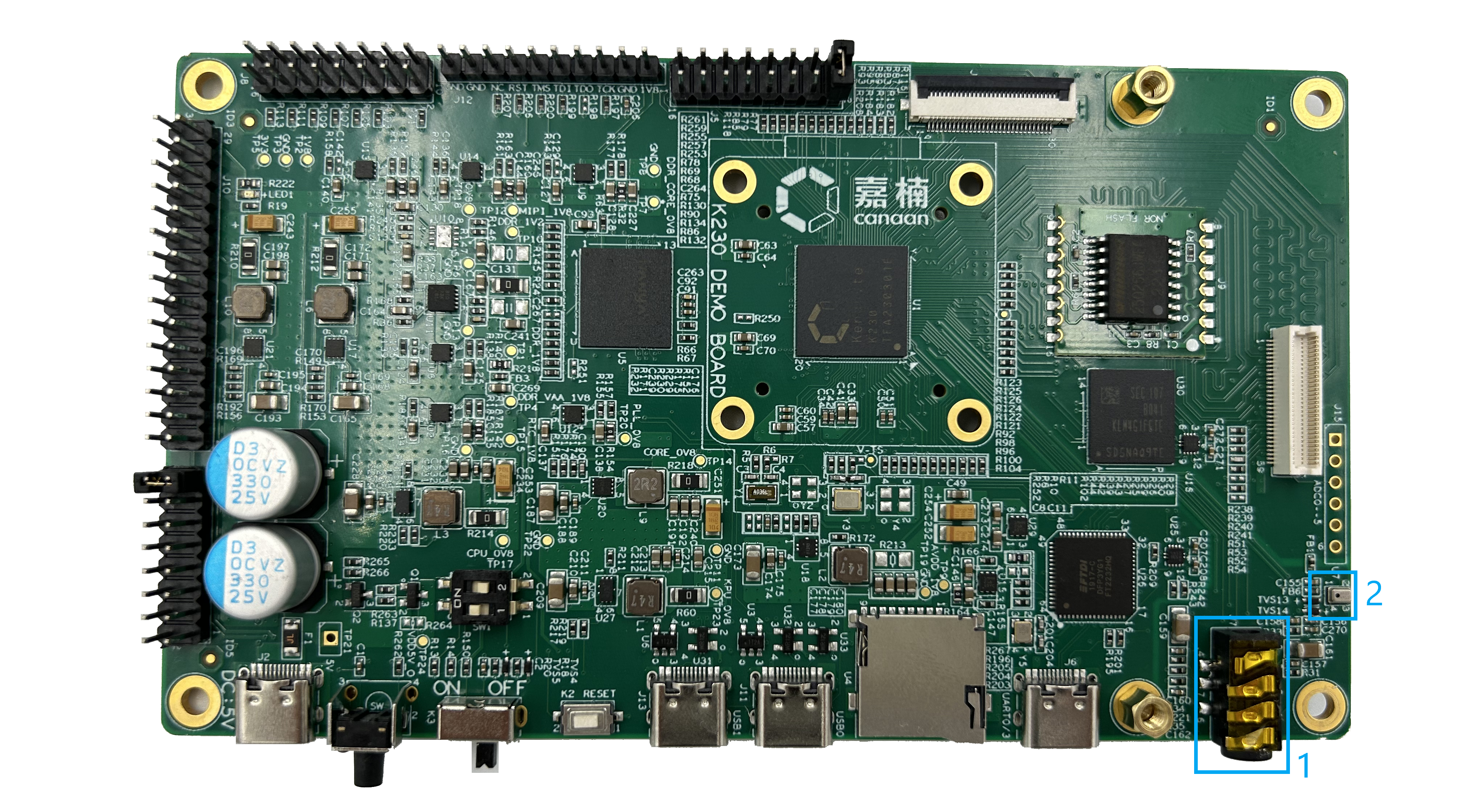
(FIGURE 2.5.1: POSITION OF HEADPHONES AND MICROPHONES ON THE DEMO BOARD).
The area of the external audio device, where the sound signal processing has been completed in the K230, can be directly connected to the headphones to output analog signals without modification. This block is only available for analog signals, and digital sound signals are led out of the header pins and externally converted externally through the I2S/PDM interface digital audio adapter board, which will be described separately in Section 2.7. The numbers in Figure 2.5.1 correspond to the following two main interfaces/devices (names are consistent with the list in the right figure in Figure 2.1.1):
HEADPHONES (PART NUMBER ON DEMO BOARD: J7)
MICROPHONE (PART NUMBER ON DEMO BOARD: U29)
Common Interface (General Development Methodology)#
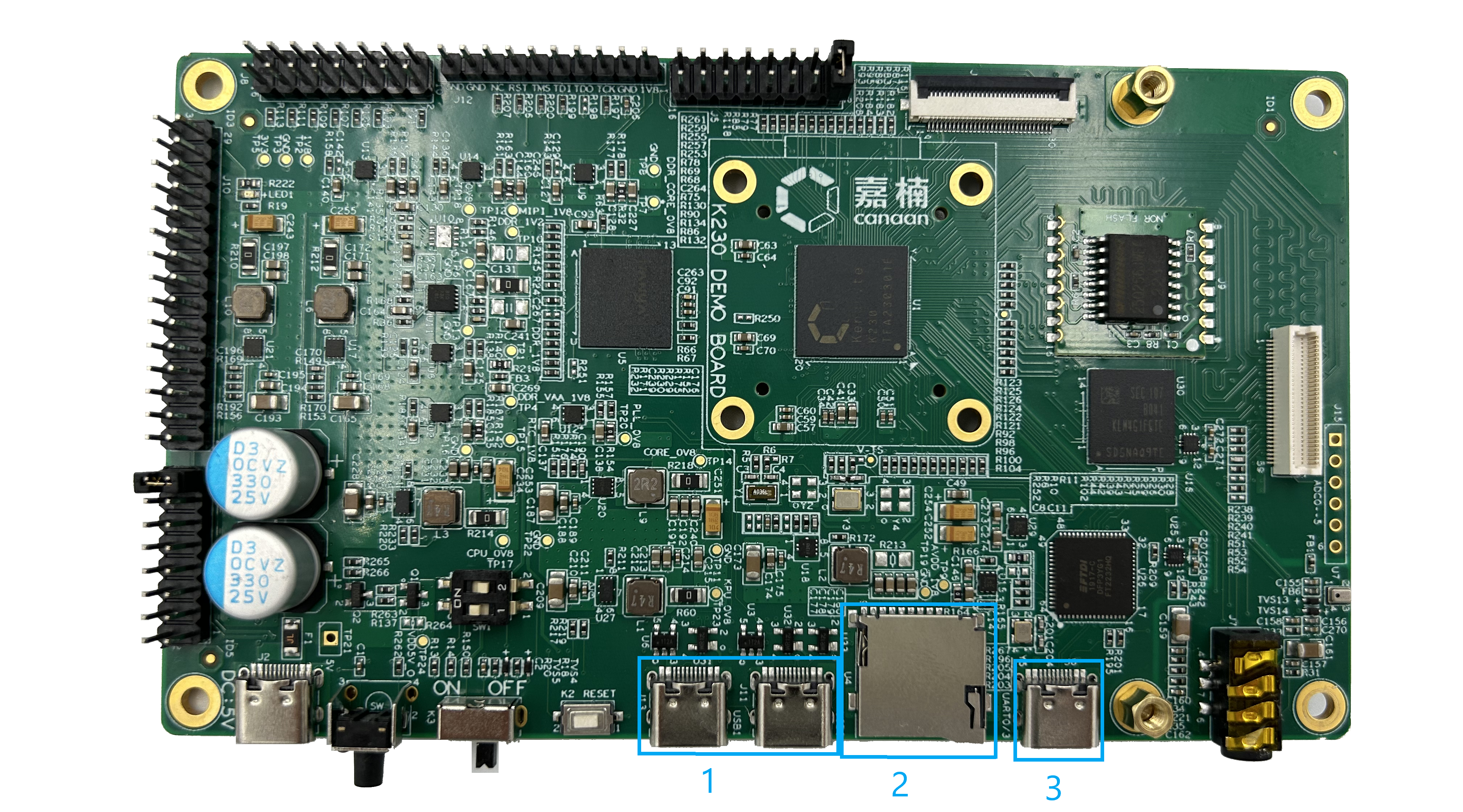 (FIGURE 2.6.1: LOCATION OF THE DATA INTERFACE ON THE DEMO BOARD).
Where the connection port to the external computer/information source is concentrated. The numbers in Figure 2.6.1 correspond to the following three main interfaces/devices (names are consistent with the list in the right figure in Figure 2.1.1):
USB 2.0 (DEMO BOARD: J11, J13). A total of two USB 2.0 interfaces supporting OTG interact directly with the K230. J11 corresponds to USB0 and J13 corresponds to USB1.
TF CARD SLOT/WIFI EXTENSION (DEVICE NUMBER ON DEMO BOARD: U4). The K230 supports booting from the TF card slot, here is where the K230 bootloader TF card is loaded. The way to choose to boot from a TF card is described in Chapter 2.3. In addition, the card slot can be connected to the WIFI daughter card described in the list of Section 1.3, and the two are multiplexed relationships. The WIFI daughter card is used to add a WIFI module to the board to verify the networking function. The daughter card has a TF card slot gold finger, which can be used normally by directly inserting the TF card slot.
SERIAL PORT DEBUGGING (DEVICE NUMBER ON DEMO BOARD: J6). Use Type C data cable for UART serial port debugging, and the serial port rate is 115200 by default.
Pin header#
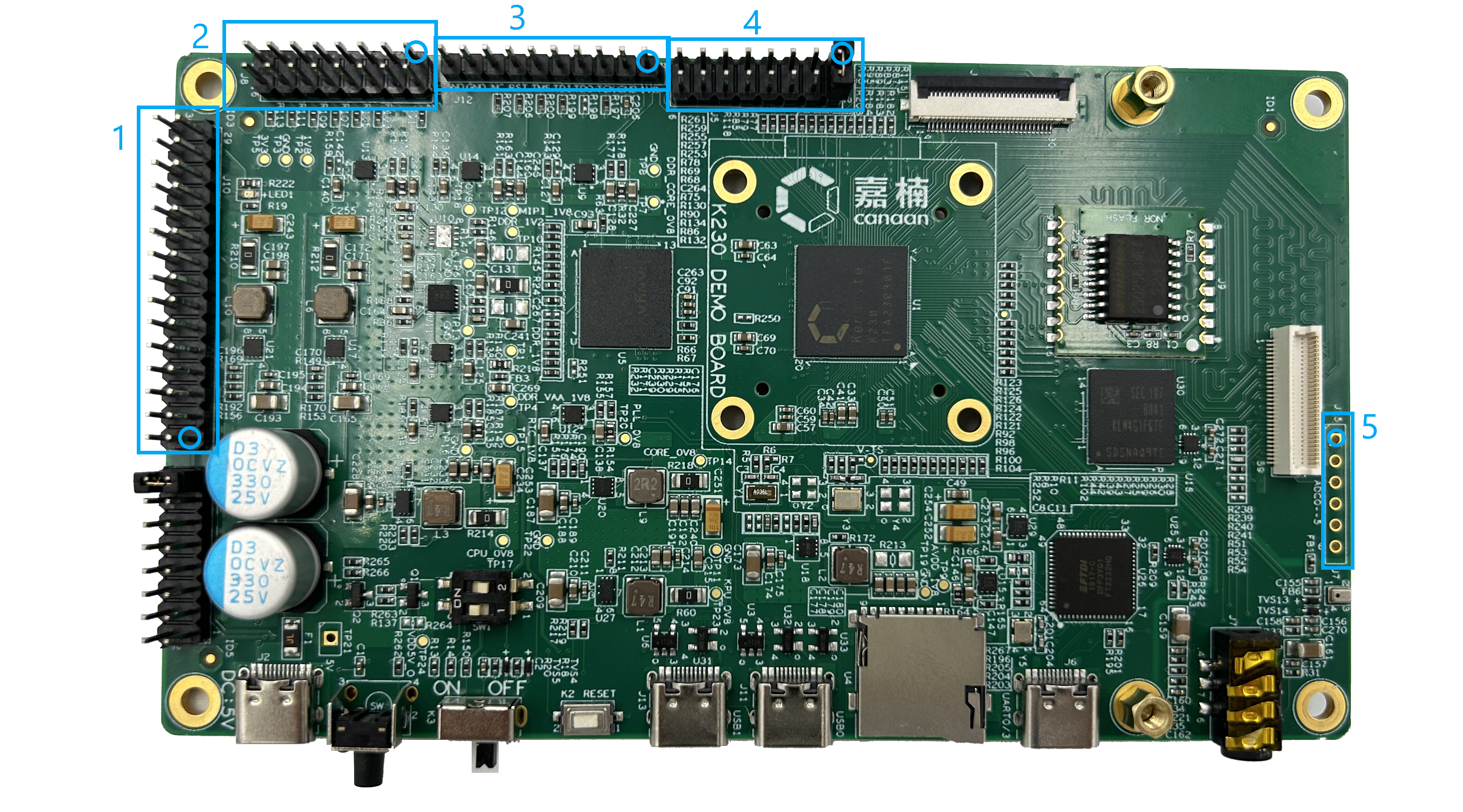 (FIG. 2.7.1: POSITION OF PIN HEADERS ON THE DEMO BOARD, PIN 1 OF EACH PIN HEADER IS CIRCLED).
The power supply on the board and some of the signal from the K230 GPIO are connected through the pin headers here. The numbers in Figure 2.7.1 correspond to the following three main interfaces/devices (names are consistent with the list in the right figure in Figure 2.1.1):
POWER MONITORING EXTENSION (PART NUMBER J10 ON DEMO BOARD). It is an internal test interface during R&D, and does not need to be used when using K230 for product development.
SDIO/I2S/PDM/IOMUX EXTENSION (PART NUMBER J8 ON DEMO BOARD). The pin header connected to the GPIO26-37 on the K230 corresponds to an IO level voltage of 1.8V. As mentioned in Section 2.5 above, the I2S/PDM interface digital audio adapter board in the daughter card list described in Section 1.3 should be placed here for external digital-to-analog conversion of the digital audio generated by the K230. Align the daughter board’s female header with pin header pin 1 here and use it on the buckle. The pin definitions are detailed in their schematics.
 (Figure 2.7.2: Schematic of SDIO/I2S/PDM/IOMUX Extension-J8).
JTAG EXTENSION (PART NUMBER J12 ON DEMO BOARD). Connect the port to the JTAG debugger. When in use, use a DuPont cable to connect the pins on the JTAG extension to the corresponding JTAG debugger port. Its pins are defined in Figure 2.7.4
 (Figure 2.7.3: Pin-defined schematic for JTAG extension with data lines pulled up to 1.8V through 10K resistors).
IOMUX/Power Extension (J5 on DEMO BOARD). The control pin of the USB and serial ports can change the mode of the two USB interfaces mentioned in Section 2.6 by shorting the J5 part pins. The pin definition for J5 is shown in Figure 2.7.5 If USB0 is required as HOST, or when used to transfer to Ethernet, pin 1,2 of J5 needs to be shortened with a jumper cap, and pin 1,2 is kept open when used as DEVICE. (Shorted by default at the time of delivery) Correspondingly, USB1 is used as HOST, or when used to convert to Ethernet, add jumping caps on pins 3 and 4 of J5. (Not shorted by default when delivered) In addition, pins 8 and 10 can be used as additional debug serial ports with UART_RX and UART_TX, respectively.
 (Figure 2.7.4: Schematic of IOMUX/Power Extension-J5).
ADC extension (J15 on demo board). The K230 has a total of 6 ADC inputs leading out to J15, which can collect sensor data or feedback signals according to the needs of the application. The input location of the ADC is located next to the MIPI CSI interface. Please note that ADC5 (the second hole in the lower right of Figure 2.7.1) is multiplexed with the headphones, and the ADC input will always be grounded and cannot be used properly when the headphones are not connected. If ADC5 does not read, plug the headphones into the headphone jack.